- 您现在的位置:买卖IC网 > Sheet目录512 > SI5935DC-T1-GE3 (Vishay Siliconix)MOSFET DUAL P-CH 20V 1206-8
AN812
Vishay Siliconix
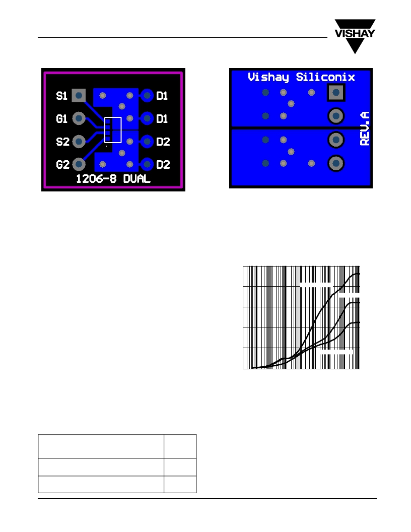
Front of Board
ChipFET r
FIGURE 3.
Back of Board
vishay.com
160
THERMAL PERFORMANCE
Junction-to-Foot Thermal Resistance (the Package
Performance)
Thermal performance for the 1206-8 ChipFET measured as
junction-to-foot thermal resistance is 30 _ C/W typical, 40 _ C/W
maximum for the dual device. The “foot” is the drain lead of the
device as it connects with the body. This is identical to the dual
SO-8 package R Q jf performance, a feat made possible by
shortening the leads to the point where they become only a
small part of the total footprint area.
The results show that a major reduction can be made in the
thermal resistance by increasing the copper drain area. In this
example, a 57 _ C/W reduction was achieved without having to
increase the size of the board. If increasing board size is an
option, a further 38 _ C/W reduction was obtained by
maximizing the copper from the drain on the larger 1” square
PCB.
200
Min. Footprint
Junction-to-Ambient Thermal Resistance
(dependent on pcb size)
The typical R Q ja for the dual-channel 1206-8 ChipFET is
90 _ C/W steady state, identical to the SO-8. Maximum ratings
are 110 _ C/W for both the 1206-8 and the SO-8. Both packages
have comparable thermal performance on the 1” square pcb
footprint with the 1206-8 dual package having a quarter of the
body area, a significant factor when considering board area.
Testing
120
80
40
Dual EVB
1” Square PCB
To aid comparison further, Figure 4 illustrates ChipFET 1206-8
dual thermal performance on two different board sizes and
three different pad patterns.The results display the thermal
performance out to steady state and produce a graphic
account on how an increased copper pad area for the drain
connections can enhance thermal performance. The
measured steady state values of R Q ja for the Dual 1206-8
ChipFET are :
1) Minimum recommended pad pattern (see 185 _ C/W
Figure 2) on the evaluation board size of
0.5 in x 0.6 in.
2) The evaluation board with the pad pattern 128 _ C/W
described on Figure 3.
0
10 -5 10 -4 10 -3 10 -2 10 -1 1 10 100 1000
Time (Secs)
FIGURE 4. Dual 1206-8 ChipFET
SUMMARY
The thermal results for the dual-channel 1206-8 ChipFET
package display identical power dissipation performance to
the SO-8 with a footprint reduction of 80%. Careful design of
the package has allowed for this performance to be achieved.
The short leads allow the die size to be maximized and thermal
resistance to be reduced within the confines of the TSOP-6
body size.
ASSOCIATED DOCUMENT
3) Industry standard 1” square pcb with
maximum copper both sides.
www.vishay.com
2
90 _ C/W
1206-8 ChipFET Single Thermal performance, AN811,
(http://www.vishay.com/doc?71126) .
Document Number: 71127
12-Dec-03
发布紧急采购,3分钟左右您将得到回复。
相关PDF资料
SI5943DU-T1-GE3
MOSFET DUAL P-CH 12V 6A 8PWRPAK
SI5975DC-T1-GE3
MOSFET 2P-CH 12V 3.1A CHIPFET
SI5980DU-T1-GE3
MOSFET N-CH 100V PPAK CHIPFET
SI6404DQ-T1-GE3
MOSFET N-CH 30V 8.6A 8TSSOP
SI6413DQ-T1-E3
MOSFET P-CH 20V 7.2A 8TSSOP
SI6423DQ-T1-GE3
MOSFET P-CH 12V 8.2A 8-TSSOP
SI6466ADQ-T1-GE3
MOSFET N-CH 20V 6.8A 8TSSOP
SI6467BDQ-T1-GE3
MOSFET P-CH 12V 6.8A 8TSSOP
相关代理商/技术参数
SI5936DU-T1-GE3
功能描述:MOSFET 30V 6.0A 10.4W 30mOhm @ 10V
RoHS:否 制造商:STMicroelectronics 晶体管极性:N-Channel 汲极/源极击穿电压:650 V 闸/源击穿电压:25 V 漏极连续电流:130 A 电阻汲极/源极 RDS(导通):0.014 Ohms 配置:Single 最大工作温度: 安装风格:Through Hole 封装 / 箱体:Max247 封装:Tube
SI5938DU
制造商:VISHAY 制造商全称:Vishay Siliconix 功能描述:Dual N-Channel 20-V (D-S) MOSFET
SI5938DU-T1-E3
功能描述:MOSFET 20V 6.0A 8.3W RoHS:否 制造商:STMicroelectronics 晶体管极性:N-Channel 汲极/源极击穿电压:650 V 闸/源击穿电压:25 V 漏极连续电流:130 A 电阻汲极/源极 RDS(导通):0.014 Ohms 配置:Single 最大工作温度: 安装风格:Through Hole 封装 / 箱体:Max247 封装:Tube
SI5938DU-T1-GE3
功能描述:MOSFET 20V 6.0A 8.3W 39mohm @ 4.5V RoHS:否 制造商:STMicroelectronics 晶体管极性:N-Channel 汲极/源极击穿电压:650 V 闸/源击穿电压:25 V 漏极连续电流:130 A 电阻汲极/源极 RDS(导通):0.014 Ohms 配置:Single 最大工作温度: 安装风格:Through Hole 封装 / 箱体:Max247 封装:Tube
SI5941DU
制造商:VISHAY 制造商全称:Vishay Siliconix 功能描述:Dual P-Channel 8-V (D-S) MOSFET
SI5943DU
制造商:VISHAY 制造商全称:Vishay Siliconix 功能描述:Dual P-Channel 12-V (D-S) MOSFET
SI5943DU-T1-E3
功能描述:MOSFET DUAL P-CH 12V(D-S) RoHS:否 制造商:STMicroelectronics 晶体管极性:N-Channel 汲极/源极击穿电压:650 V 闸/源击穿电压:25 V 漏极连续电流:130 A 电阻汲极/源极 RDS(导通):0.014 Ohms 配置:Single 最大工作温度: 安装风格:Through Hole 封装 / 箱体:Max247 封装:Tube
SI5943DU-T1-GE3
功能描述:MOSFET 12V 6.0A 8.3W 64mohm @ 4.5V RoHS:否 制造商:STMicroelectronics 晶体管极性:N-Channel 汲极/源极击穿电压:650 V 闸/源击穿电压:25 V 漏极连续电流:130 A 电阻汲极/源极 RDS(导通):0.014 Ohms 配置:Single 最大工作温度: 安装风格:Through Hole 封装 / 箱体:Max247 封装:Tube